TLDR 🔗
This tool converts SVG vector graphics to Cadsoft Eagle polygon. Get it here.
Why 🔗
Technology can even in its most raw and bare form certainly be beautiful. The bottom of a motherboard, with long, parallell, impedance-matched traces from PCI-connectors is a good example. A large BGA is another, with traces extending in every direction.
I've long wanted to make my PCBs more beautiful, taking the few "colors" into full use. By chosing carefully where you have soldermask, no soldermask, silkscreen, copper, etc, you actually get a few dimensions to play with.

I use Cadsoft Eagle for my designs, not because it's particularly stellar, but because it's one of the least bad alternatives, it's free, files are in XML-format, but perhaps most importantly, because I used it in school and had to climb that steep learning curve. Eagle has crappy support for using external files or graphics. There are plugins that you can download that imports 2-bit bmp's, that creates a small rectangle fill for each pixel. Not very user friendly, not very efficient, not very nice. I want vector graphics with nice bezier curves and scalability properties. There is a plugin (an .ulp) for that, but when I tried it, it didn't work although I was closely following the instructions. And, I couldn't understand why, because the .ulp uses Eagle-specific code that I didn't want to sink time into learning. To be fair, I didn't look more than a few seconds on the code.
SVG parser tool 🔗
So I wrote a new tool for myself. It parses a SVG vector graphics file (from eg Inkscape) and creates a script that when run in Eagle creates a set of polygons at any given size and rotation and so on.
You can find it, together with instructions on how to use it, on my github repo: https://github.com/msloth/eagle-poly-from-vgfx
How to 🔗
Here's an guide through images on how to use it.
First, start with a picture. I like William Gibson so here's Johnny Mnemonic.

Then, I mirrored it (cause I wanted to) and made it black and white.


Then, I worked it up really good with Inkscape to get a vector graphics image. Save it as a "plain SVG" (in Inkscape).

Next, treat it according to the instructions you find in the README in the repo (removing curves etc).
Run the tool over it. Now we have a Eagle script that will create the polygons needed.
Start Eagle. Open your project. Switch to board design view. Run the script we just created menues -> "Run user script…".
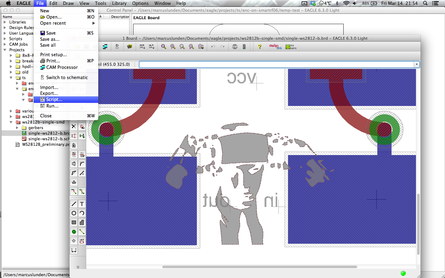
This creates polygons from the image. These can be put on the silk screen layer, or as I did, put it on the Top copper layer. To make the metal show, we also have an exact copy of the polygon but on the tStop layer. Chosing layers etc are done when you run the tool, not in Eagle.
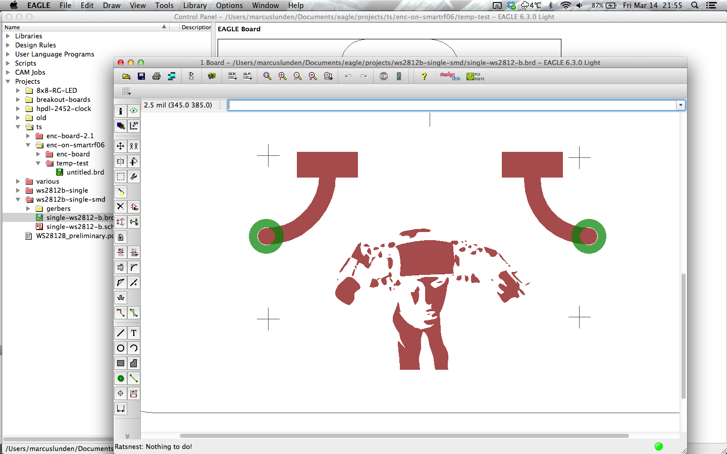
Create the Gerbers, just as you would normally do. Verify them using some Gerber viewer. Send it to e.g. OSHpark or Seeedstudio.
Enjoy the results.
